
Design Rules for Rigid-Flex PCB Fabrication
Rigid-Flex PCB Fabrication
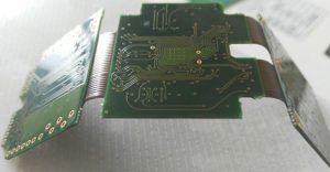
Rigid-flex PCBs offer the best of both rigid and flexible circuit board design, allowing manufacturers to maneuver complex boards in tight spaces while providing superior reliability. These circuits require special lamination, drilling and routing processes as well as careful inspection. As a result, rigid-flex boards can be expensive. To mitigate these costs, it is critical to understand the design rules that are crucial to follow in rigid-flex PCB fabrication. These include design rules based on thickness and bend radius, stackup, traces, impedance, and vias.
The layered structure of rigid flex pcb fabrication is usually comprised of a core and a conductive layer. The core is usually made of polyimide or FR4. Rigid-flex PCBs can be manufactured with different materials and constructions, but the most popular are single-sided, double-sided, four-layer, and multilayer. They can also have copper traces and pads on both sides of the board, as well as power and ground planes.
Traces should be spaced far enough apart to prevent them from overlapping in the same area. This will minimize the stress on the traces during bending and ensure that they don’t get stuck or damaged. It is also important to keep traces away from the edges of the flexible sections of the board, as these will cause mechanical stresses that can break or damage the components. This can be achieved by using dummy traces or by placing them on the innermost layers of the flex section.
Design Rules for Rigid-Flex PCB Fabrication
It is vital to have a large enough bending radius in the flexible areas of a flex PCB. This will reduce the possibility of cracking or damaging the copper traces. The optimum bending radius will vary depending on the thickness of the flex section and the dynamic shapeability requirements of the board. The bending radius should be at least 6 times the thickness of the flexible composite.
A high-quality flex circuit requires a precise stackup that balances factors such as flexibility, stiffness, thickness, and impedance control. The stackup should contain enough rigid layers to support component leads and a flex section that is at least as thick as the rigid layer. It is also important to consider whether the stackup should use panel plating or pad-only plating (button plating). Panel plating allows for higher etch yields, but it is more difficult to achieve controlled impedance.
Another factor that affects the flex PCB’s flexibility is the amount of copper that is used. A thin copper stack-up will provide more flexibility, while a thicker one will be more rigid. It is also important to choose a suitable surface finish, as this will improve solderability and prevent copper oxidation.
Rigid-flex PCBs are increasingly being used in mobile phones, wearable devices, and other electronic devices that need to be foldable or able to bend. They are also being used in aerospace systems, as conformal heating elements, and in medical applications for health and safety monitoring. As a result, it is critical to understand the design rules for rigid-flex PCBs in order to produce quality boards that meet all of the necessary specifications.
